|
Gallium Nitride on Sapphire Substrate |
|||||||||||||||||||||||||||||||||||||||||||||||||||||||||||||||||||||||||||||||||||||||||||||||||||||||||||||||||||||||||||||||||||||||||||||||||||||||||||||||||||||||||||||||||||||||||||||||||||||||||||||||||||||||||||||||||||||||||||||||||||||||||||||||||||||||||||||||||||||||||||||||||||||||||||||||||||||||||||||||||||||||||||||||||||||||||
|
Micro LEDs are considered a key technology for the metaverse platform for enabling next-generation displays for augmented reality (AR), virtual reality (VR), mobile phones, and smart watches.
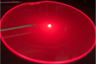
GaN based Red LED (610~680nm) Epitaxial Wafers:
4 Inch intrinsic GaN GaN Epitaxial template on sapphire:
4 Inch intrinsic GaN Epitxial template on sapphire in stock, 300nm GaN thickness, double side polished sapphire substrate, PWGS-13563A211($860.0):
4 Inch intrinsic GaN Epitxial template on sapphire in stock, 100nm GaN thickness, double side polished sapphire substrate, PWGS-13573A211($830.0):
4 Inch intrinsic GaN Epitxial template on sapphire in stock, 100nm GaN thickness, single side polished sapphire substrate, PWGS-13573A111($800.0):
2 Inch Si-doped N-Type GaN Epitaxial template on sapphire:
2 Inch Si-doped GaN Epitxial template on sapphire in stock, single side polished, PWGS-111132111($365.0):
2 Inch Si-doped GaN Epitxial template on sapphire in stock, double side polished, PWGS-111132211($385.0):
2 Inch Mg-doped P-Type GaN Epitaxial template on sapphire:
2 Inch Mg-doped GaN Epitxial template on sapphire in stock, single side polished, PWGS-11123A111($266.0):
2 Inch Mg-doped GaN Epitxial template on sapphire in stock, double side polished, PWGS-11123A211($268.0):
Doped GaN Epitxial on Sapphire for Blue/Green/UV-LED:
2 inch 375nm UV Epi-wafer in stock, C-plane sapphire substrate, Single side polished, PWGS-11063A111($950.0):
2 inch GaN based green Epi-wafer, 4.0um thick GaN Epi-layer on C-plane sapphire substrate in stock, Single side polished, PWGS-11233A111($160.0):
2 inch GaN based green Epi-wafer, 4.0um thick GaN Epi-layer on C-plane sapphire substrate in stock, double side polished, PWGS-11233A211($186.0):
2 inch GaN based blue Epi-wafer, 6.2um thick GaN Epi-layer on C-plane patterned sapphire substrate in stock, single side polished, PWGS-11443A111($186.0):
2 inch GaN based blue Epi-wafer, 5.6um thick GaN Epi-layer on C-plane sapphire substrate in stock, double side polished, PWGS-11363A211($192.0):
4 inch GaN based green Epi-wafer, 5.5um thick GaN Epi-layer on C-plane sapphire substrate in stock, double side polished, PWGS-13053A211($296.0):
4 inch GaN based green Epi-wafer, 6.3um thick GaN Epi-layer on patterned sapphire substrate in stock, single side polished, PWGS-13053A311($268.0):
4 inch GaN based blue Epi-wafer, 5.6um thick GaN Epi-layer on C-plane sapphire substrate in stock, double side polished, PWGS-13363A211($296.0):
4 inch GaN based 495nm emission wavelength Epi-wafer on C-plane sapphire substrate in stock, double side polished, PWGS-13083A211($312.0):
4 inch GaN based 495nm emission wavelength Epi-wafer on patterned sapphire substrate in stock, single side polished, PWGS-13053A311($290.0):
|
|||||||||||||||||||||||||||||||||||||||||||||||||||||||||||||||||||||||||||||||||||||||||||||||||||||||||||||||||||||||||||||||||||||||||||||||||||||||||||||||||||||||||||||||||||||||||||||||||||||||||||||||||||||||||||||||||||||||||||||||||||||||||||||||||||||||||||||||||||||||||||||||||||||||||||||||||||||||||||||||||||||||||||||||||||||||||

Copyright © 2016 Precision Micro-Optics Inc. All Rights Reserved.