|
Intersubband Transitions |
|||||||||||||||||||||||||||||||||||||||||||||||||||||
|
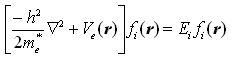
Description: Intersubband transitions in semiconductor quantum wells (QWs) have been the subject of extensive research for the past several decades. The wide conduction band offset such as GaN/AlGaN heterostructs has extended the transitions into near infrared region. Quantum cascade laser and quantum-well infrared photodetector are two successfully commercialized products. To design a desired QW structure and improve a device performance, a numerical simulation is needed to compute the energy levels and corresponding envelope functions, the intersubband transition dipole moments, carrier densities, relaxation times and other parameters 1. Numerical solution of the Self-Consistent Poisson and Schrödinger Equations The Schrödinger equation for the envelope function based on the effective-mass approximation is given:
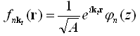
If the spatial coordinate z is chosen as growth direction, the free motion in the x-y plane can be separated as follows:
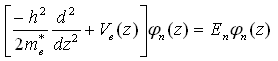
where k t denotes the two-dimensional vector (k x ,k y). The Schrödinger equation is simplified as:
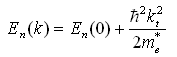
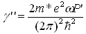
where me* : Effective mass φn(z) : Envelope function of the n-th subband En(0) : n-th subband energy at k t=0 Vbi(z) : Built-in potential VH(z) : Hartree potential
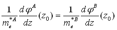
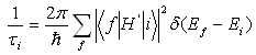
The envelope-function Schrödinger equation is able to be solved independently in each layer of the heterostructure by using a propagation matrix approach, and the solutions are then connected to one another with the matching conditions (6, 7) at each interface z0. To reach a self-consistent set of solutions, the Schrödinger equation is first solved by neglecting the Hartree potential contribution; the calculated envelope functions are then used in the Poisson equation to determine the electrostatic potential and therefore the Hartree potential energy; this is then used to find an updated set of solutions of the Schrödinger equation, and so forth until the calculated bound-state energies converge. 2.Longitudinal Optical Phonon Scattering The non-radiative intersubband relaxation rate is typically dominated by LO-phonon scattering processes. The calculation is based on Fermi’s golden rule, which states that the probability per unit time that an electron in an initial state |i> of energy Ei is scattered by a time-dependent perturbation H' into a final state |f> of energy Ef is given:
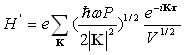
where ω : LO-Photon angular frequency K : LO-Photon wave vector ε∞ : High frequency permittivities of the material εs : Low frequency permittivities of the material The time-dependent perturbation H' induced by atom vibration represents the crystal potential energy which can scatter the mobile charge carriers within the crystal. Through a tedious calculation, the scattering rate in a QW structure can then be written as:
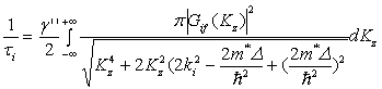
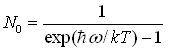
where Gif(Kz) : Form factor N0 : LO-phonon number given by Bose-Einstein distribution In the Δ=Ef-Ei±ħω, the lower sign represents absorption which reduces the phonon population by 1, while the upper sign represents emission which increases the number of phonons by 1. 3.Modeling of Intersubband Transitions A TM mode optical pulse launched into a QW structure undergoes the absorption. The process can be studied using the following rate equations for two-level QW system, which are derived from a standard model of nonlinear optics in the two-level approximation.
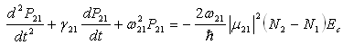
where N1 and N2 : Electron density of the two subbands Ec : Electrical field of the optical wave P21: Induced polarization density associated with the transition between two subbands τ21 : Relaxation time from |2> to |1> μ21 : Dipole moment ħγ21 : Full width at half maximum (FWHM) of the |2> to |1> transition The rate equations could be solved in the time domain using a finite-difference method. At each time step, the instantaneous subband populations computed from these equations are used in the Poisson-Schrödinger solver to calculate energy levels, dipole moments and relaxation lifetimes at that time; these parameters are then fed back into the rate equations to find the carrier densities at the next time step, and so forth. Features:
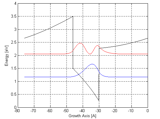
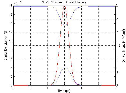
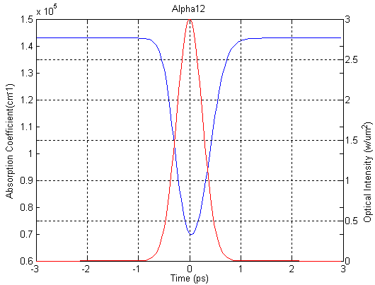
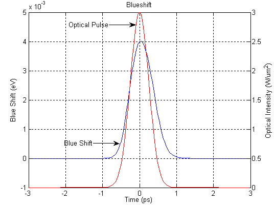
Example: Cross-absorption Modulation in a Two-level System This example considers a QW structure consisting of a 16-Å GaN well separated by 30-Å AlN barriers, with a doping density of 3E19 cm-3 in the barriers. Simulation results describing cross-absorption modulation in this structure are presented in following figures, for a case of a Gaussian pulse of carrier frequency ωc=ω21, temporal width 1ps, and peak intensity 3.0W/um2. Figure 1 shows a calculated conduction-band diagram and bound states. The band tilting is created by built-in electric fields of GN/AlN heterostructure due to the presence of strong spontaneous and piezoelectric polarizations in nitride semiconductors, whose discontinuities at each heterojunction leading to large densities of interface charge. Figure 2 indicates carrier densities of the ground-state subband |1> and the upper subband |2> at the presence of a Gaussian pulse in red color. The carrier redistribution produces a stark blue shift indicated in figure 4. Meanwhile the redistribution and the blue shift lead to absorption saturation shown in figure 3.
Bibliography: [1] S.L. Chuang Physics of Optoelectronics(1995) [2] R.W. Boyd Nonlinear Optics (1992) [3] P.Harrison Quantum Wells, Wires and Dots (2000) |
||||||||||||||||||||||||||||||||||||||||||||||||||||||

Copyright © 2016 Precision Micro-Optics Inc. All Rights Reserved.